 | –≠–ª–µ–∫—Ç—Ä–æ–Ω–Ω—ã–π –∫–æ–º–ø–æ–Ω–µ–Ω—Ç: TNY267G | –°–∫–∞—á–∞—Ç—å:  PDF PDF  ZIP ZIP |
TNY264/266-268
TinySwitch-II
Family
Enhanced, Energy Efficient,
Low Power Off-line Switcher
Æ
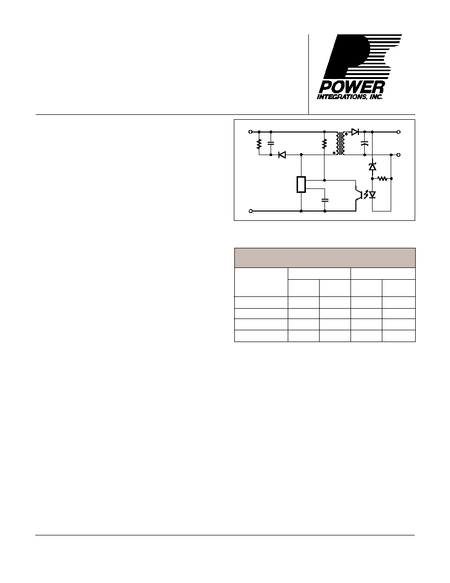
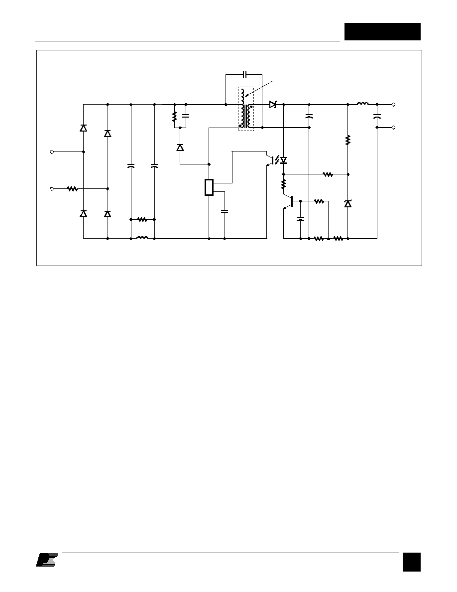
Figure 1. Typical Standby Application.
Product Highlights
TinySwitch-II
Features Reduce System Cost
∑ Fully integrated auto-restart for short circuit and open
loop fault protection≠saves external component costs
∑ Built-in circuitry practically eliminates audible noise with
ordinary varnished transformer
∑ Programmable line under-voltage detect feature prevents
power on/off glitches≠saves external components
∑ Frequency jittering dramatically reduces EMI (~10 dB)
≠minimizes EMI filter component costs
∑ 132 kHz operation reduces transformer size≠allows use of
EF12.6 or EE13 cores for low cost and small size
∑ Very tight tolerances and negligible temperature variation
on key parameters eases design and lowers cost
∑ Lowest component count switcher solution
Better Cost/Performance over RCC & Linears
∑ Lower system cost than RCC, discrete PWM and other
integrated/hybrid solutions
∑ Cost effective replacement for bulky regulated linears
∑ Simple ON/OFF control≠no loop compensation needed
∑ No bias winding≠simpler, lower cost transformer
EcoSmart
Æ
≠Extremely Energy Efficient
∑ No load consumption < 50 mW with bias winding and
< 250 mW without bias winding at 265 VAC input
∑ Meets Blue Angel, Energy Star, and EC requirements
∑ Ideal for cell-phone charger and PC standby applications
High Performance at Low Cost
∑ High voltage powered≠ideal for charger applications
∑ High bandwidth provides fast turn on with no overshoot
∑ Current limit operation rejects line frequency ripple
∑ Built-in current limit and thermal protection
Description
TinySwitch-II maintains the simplicity of the TinySwitch
topology, while providing a number of new enhancements to
further reduce system cost and component count, and to
practically eliminate audible noise. Like TinySwitch, a 700 V
power MOSFET, oscillator, high voltage switched current source,
current limit and thermal shutdown circuitry are integrated onto a
monolithic device. The start-up and operating power are derived
directly from the voltage on the DRAIN pin, eliminating the
need for a bias winding and associated circuitry. In addition, the
PI-2684-101700
Wide-Range
HV DC Input
D
S
EN/UV
BP
+
-
+
-
DC Output
TinySwitch-II
Optional
UV Resistor
Æ
July 2001
PRODUCT
(3)
Adapter
(1)
Open
Frame
(2)
Open
Frame
(2)
OUTPUT POWER TABLE
Table 1. Notes: 1. Typical continuous power in a non-ventilated enclosed
adapter measured at 50 ∞C ambient. 2. Maximum practical continuous
power in an open frame design with adequate heat sinking, measured at
50 ∞C ambient (See key applications section for details). 3. Packages:
P: DIP-8B, G: SMD-8B. Please see part ordering information.
230 VAC
±
15%
Adapter
(1)
85-265 VAC
5.5 W
9 W
4 W
6 W
10 W
15 W
6 W
9.5 W
13 W
19 W
8 W
12 W
16 W
23 W
10 W
15 W
TNY264P or G
TNY266P or G
TNY267P or G
TNY268P or G
TinySwitch-II devices incorporate auto-restart, line under-
voltage sense, and frequency jittering. An innovative design
minimizes audio frequency components in the simple ON/OFF
control scheme to practically eliminate audible noise with
standard taped/varnished transformer construction. The fully
integrated auto-restart circuit safely limits output power during
fault conditions such as output short circuit or open loop,
reducing component count and secondary feedback circuitry
cost. An optional line sense resistor externally programs a line
under-voltage threshold, which eliminates power down glitches
caused by the slow discharge of input storage capacitors present
in applications such as standby supplies. The operating frequency
of 132 kHz is jittered to significantly reduce both the quasi-peak
and average EMI, minimizing filtering cost.
2
B
7/01
TNY264/266-268
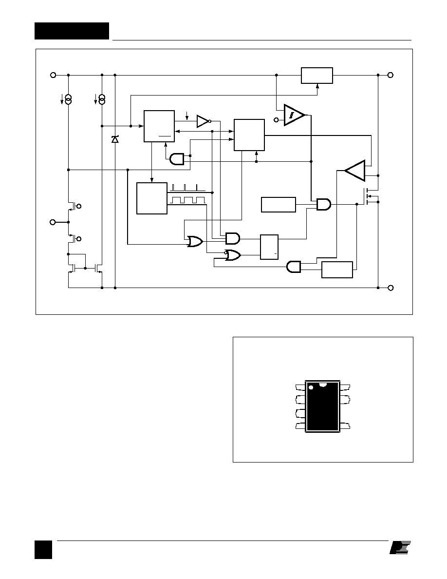
Figure 2. Functional Block Diagram.
Figure 3. Pin Configuration.
Pin Functional Description
DRAIN (D) Pin:
Power MOSFET drain connection. Provides internal operating
current for both start-up and steady-state operation.
BYPASS (BP) Pin:
Connection point for a 0.1
µF external bypass capacitor for the
internally generated 5.8 V supply.
ENABLE/UNDER-VOLTAGE (EN/UV) Pin:
This pin has dual functions: enable input and line under-voltage
sense. During normal operation, switching of the power
MOSFET is controlled by this pin. MOSFET switching is
terminated when a current greater than 240
µA is drawn from
this pin. This pin also senses line under-voltage conditions
through an external resistor connected to the DC line voltage.
If there is no external resistor connected to this pin,
TinySwitch-II detects its absence and disables the line under-
voltage function.
SOURCE (S) Pin:
Control circuit common, internally connected to output
MOSFET source.
SOURCE (HV RTN) Pin:
Output MOSFET source connection for high voltage return.
PI-2643-030701
CLOCK
OSCILLATOR
5.8 V
4.8 V
SOURCE
(S)
S
R
Q
DCMAX
BYPASS
(BP)
+
-
VI
LIMIT
FAULT
PRESENT
CURRENT LIMIT
COMPARATOR
ENABLE
LEADING
EDGE
BLANKING
THERMAL
SHUTDOWN
+
-
DRAIN
(D)
REGULATOR
5.8 V
BYPASS PIN
UNDER-VOLTAGE
1.0 V + VT
ENABLE/
UNDER-
VOLTAGE
(EN/UV)
Q
240
µ
A
50
µ
A
LINE UNDER-VOLTAGE
RESET
AUTO-
RESTART
COUNTER
JITTER
1.0 V
6.3 V
CURRENT
LIMIT STATE
MACHINE
PI-2685-101600
EN/UV
D
S
S
S (HV RTN)
S (HV RTN)
BP
P Package (DIP-8B)
G Package (SMD-8B)
8
5
7
1
4
2
3
3
B
7/01
TNY264/266-268
TinySwitch-II
Functional Description
TinySwitch-II combines a high voltage power MOSFET switch
with a power supply controller in one device. Unlike conventional
PWM (Pulse Width Modulator) controllers, TinySwitch-II uses
a simple ON/OFF control to regulate the output voltage.
The TinySwitch-II controller consists of an Oscillator, Enable
Circuit (Sense and Logic), Current Limit State Machine, 5.8 V
Regulator, Bypass pin Under-Voltage Circuit, Over
Temperature Protection, Current Limit Circuit, Leading Edge
Blanking and a 700 V power MOSFET. TinySwitch-II
incorporates additional circuitry for Line Under-Voltage Sense,
Auto-Restart and Frequency Jitter. Figure 2 shows the functional
block diagram with the most important features.
Oscillator
The typical oscillator frequency is internally set to an average
of 132 kHz. Two signals are generated from the oscillator: the
Maximum Duty Cycle signal (DC
MAX
) and the Clock signal that
indicates the beginning of each cycle.
The TinySwitch-II oscillator incorporates circuitry that
introduces a small amount of frequency jitter, typically 8 kHz
peak-to-peak, to minimize EMI emission. The modulation rate
of the frequency jitter is set to 1 kHz to optimize EMI reduction
for both average and quasi-peak emissions. The frequency jitter
should be measured with the oscilloscope triggered at the
falling edge of the DRAIN waveform. The waveform in Figure4
illustrates the frequency jitter of the TinySwitch-II.
Enable Input and Current Limit State Machine
The enable input circuit at the EN/UV pin consists of a low
impedance source follower output set at 1.0 V. The current
through the source follower is limited to 240
µA. When the
current out of this pin exceeds 240
µA, a low logic level
(disable) is generated at the output of the enable circuit. This
enable circuit output is sampled at the beginning of each cycle
on the rising edge of the clock signal. If high, the power
MOSFET is turned on for that cycle (enabled). If low, the power
MOSFET remains off (disabled). Since the sampling is done
only at the beginning of each cycle, subsequent changes in the
EN/UV pin voltage or current during the remainder of the cycle
are ignored.
The Current Limit State Machine reduces the current limit by
discrete amounts at light loads when TinySwitch-II is likely to
switch in the audible frequency range. The lower current limit
raises the effective switching frequency above the audio range
and reduces the transformer flux density including the associated
audible noise. The state machine monitors the sequence of
EN/UV pin voltage levels to determine the load condition and
adjusts the current limit level accordingly in discrete amounts.
Under most operating conditions (except when close to no-
load), the low impedance of the source follower keeps the
voltage on the EN/UV pin from going much below 1.0 V in the
disabled state. This improves the response time of the optocoupler
that is usually connected to this pin.
5.8 V Regulator and 6.3 V Shunt Voltage Clamp
The 5.8 V regulator charges the bypass capacitor connected to
the BYPASS pin to 5.8 V by drawing a current from the voltage
on the DRAIN pin, whenever the MOSFET is off. The
BYPASS pin is the internal supply voltage node for the
TinySwitch-II. When the MOSFET is on, the TinySwitch-II
operates from the energy stored in the bypass capacitor.
Extremely low power consumption of the internal circuitry
allows TinySwitch-II to operate continuously from current it
takes from the DRAIN pin. A bypass capacitor value of 0.1
µF
is sufficient for both high frequency decoupling and energy
storage.
In addition, there is a 6.3 V shunt regulator clamping the
BYPASS pin at 6.3 V when current is provided to the BYPASS
pin through an external resistor. This facilitates powering of
TinySwitch-II externally through a bias winding to decrease the
no load consumption to about 50 mW.
BYPASS Pin Under-Voltage
The BYPASS pin under-voltage circuitry disables the power
MOSFET when the BYPASS pin voltage drops below 4.8 V.
Once the BYPASS pin voltage drops below 4.8 V, it must rise
back to 5.8 V to enable (turn-on) the power MOSFET.
Figure 4. Frequency Jitter.
PI-2741-041901
0
5
10
Time (
µ
s)
0
100
200
400
500
600
300
V
DRAIN
136 kHz
128 kHz

4
B
7/01
TNY264/266-268
Over Temperature Protection
The thermal shutdown circuitry senses the die temperature. The
threshold is typically set at 135
∞C with 70 ∞C hysteresis. When
the die temperature rises above this threshold the power
MOSFET is disabled and remains disabled until the die
temperature falls by 70
∞C, at which point it is re-enabled. A
large hysteresis of 70
∞C (typical) is provided to prevent
overheating of the PC board due to a continuous fault condition.
Current Limit
The current limit circuit senses the current in the power MOSFET.
When this current exceeds the internal threshold (I
LIMIT
), the
power MOSFET is turned off for the remainder of that cycle.
The current limit state machine reduces the current limit threshold
by discrete amounts under medium and light loads.
The leading edge blanking circuit inhibits the current limit
comparator for a short time (t
LEB
) after the power MOSFET is
turned on. This leading edge blanking time has been set so that
current spikes caused by capacitance and secondary-side rectifier
reverse recovery time will not cause premature termination of
the switching pulse.
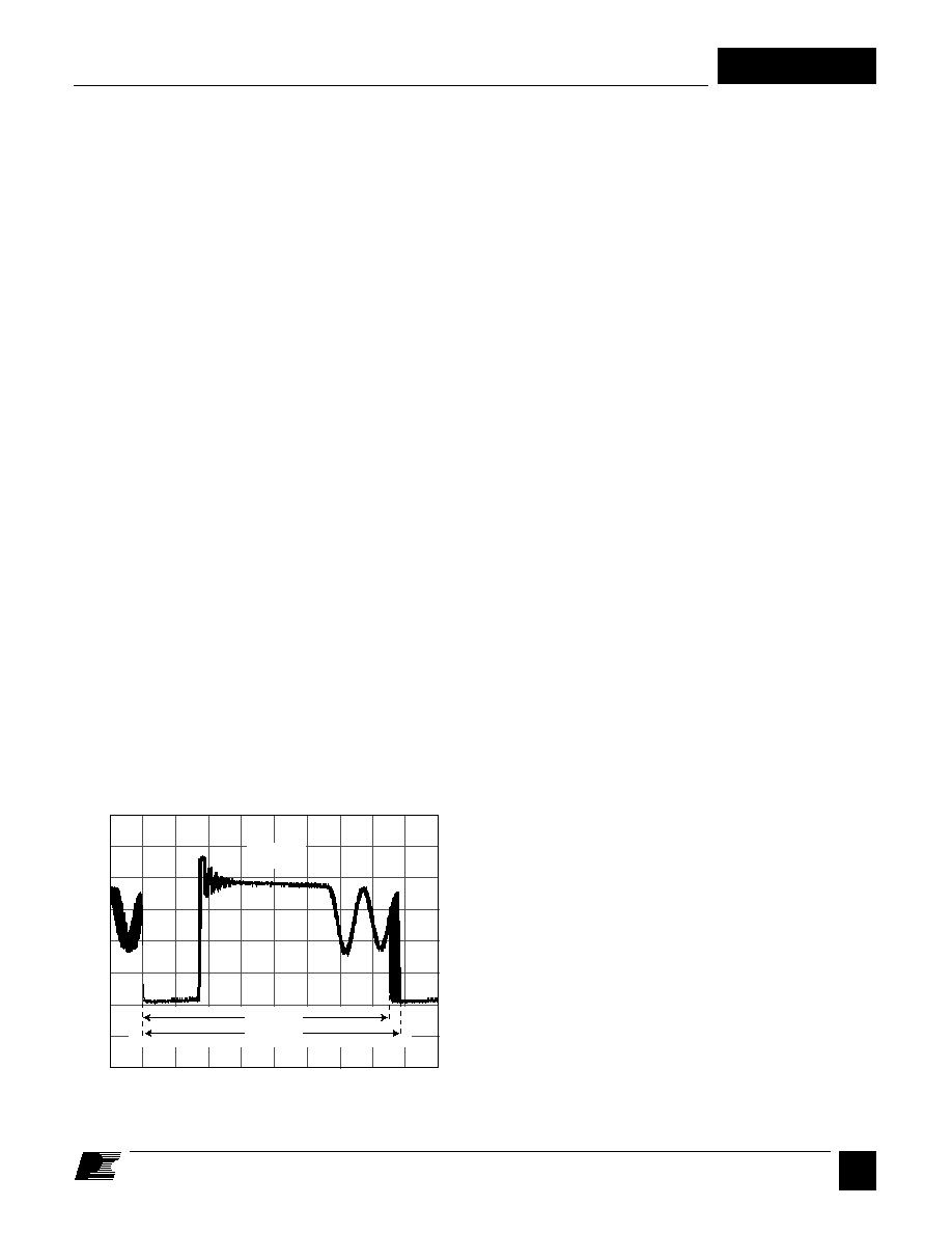
Auto-Restart
In the event of a fault condition such as output overload, output
short circuit, or an open loop condition, TinySwitch-II enters
into auto-restart operation. An internal counter clocked by the
oscillator gets reset every time the EN/UV pin is pulled low. If
the EN/UV pin is not pulled low for 50 ms, the power MOSFET
switching is normally disabled for 850 ms (except in the case of
line under-voltage condition in which case it is disabled until
the condition is removed). The auto-restart alternately enables
and disables the switching of the power MOSFET until the fault
condition is removed. Figure 5 illustrates auto-restart circuit
operation in the presence of an output short circuit.
In the event of a line under-voltage condition, the switching of
the power MOSFET is disabled beyond its normal 850 ms time
until the line under-voltage condition ends.
Line Under-Voltage Sense Circuit
The DC line voltage can be monitored by connecting an
external resistor from the DC line to the EN/UV pin. During
power-up or when the switching of the power MOSFET is
disabled in auto-restart, the current into the EN/UV pin must
exceed 50
µA to initiate switching of the power MOSFET.
During power-up, this is implemented by holding the BYPASS
pin to 4.8 V while the line under-voltage condition exists. The
BYPASS pin then rises from 4.8 V to 5.8V when the line under-
voltage condition goes away. When the switching of the power
MOSFET is disabled in auto-restart mode and a line under-
voltage condition exists, the auto-restart counter is stopped.
This stretches the disable time beyond its normal 850ms until
the line under-voltage condition ends.
The line under-voltage circuit also detects when there is no
external resistor connected to the EN/UV pin (less than ~ 2
µA
into pin). In this case the line under-voltage function is disabled.
TinySwitch-II
Operation
TinySwitch-II devices operate in the current limit mode. When
enabled, the oscillator turns the power MOSFET on at the
beginning of each cycle. The MOSFET is turned off when the
current ramps up to the current limit or when the DC
MAX
limit is
reached. As the highest current limit level and frequency of a
TinySwitch-II design are constant, the power delivered to the
load is proportional to the primary inductance of the transformer
and peak primary current squared. Hence, designing the supply
involves calculating the primary inductance of the transformer
for the maximum output power required. If the TinySwitch-II is
appropriately chosen for the power level, the current in the
calculated inductance will ramp up to current limit before the
DC
MAX
limit is reached.
Enable Function
TinySwitch-II senses the EN/UV pin to determine whether or
not to proceed with the next switch cycle as described earlier.
The sequence of cycles is used to determine the current limit.
Once a cycle is started, it always completes the cycle (even
when the EN/UV pin changes state half way through the cycle).
This operation results in a power supply in which the output
voltage ripple is determined by the output capacitor, amount of
energy per switch cycle and the delay of the feedback.
The EN/UV pin signal is generated on the secondary by
comparing the power supply output voltage with a reference
voltage. The EN/UV pin signal is high when the power supply
output voltage is less than the reference voltage.
In a typical implementation, the EN/UV pin is driven by an
optocoupler. The collector of the optocoupler transistor
isconnected to the EN/UV pin and the emitter is connected to
Figure 5. TinySwitch-II Auto-Restart Operation.
PI-2699-030701
0
1000
2000
Time (ms)
0
5
0
10
100
200
300
V
DRAIN
V
DC-OUTPUT
5
B
7/01
TNY264/266-268
V
DRAIN
V
EN
CLOCK
D
DRAIN
I
MAX
PI-2749-050301
the SOURCE pin. The optocoupler LED is connected in series
with a Zener diode across the DC output voltage to be regulated.
When the output voltage exceeds the target regulation voltage
level (optocoupler LED voltage drop plus Zener voltage), the
optocoupler LED will start to conduct, pulling the EN/UV pin
low. The Zener diode can be replaced by a TL431 reference
circuit for improved accuracy.
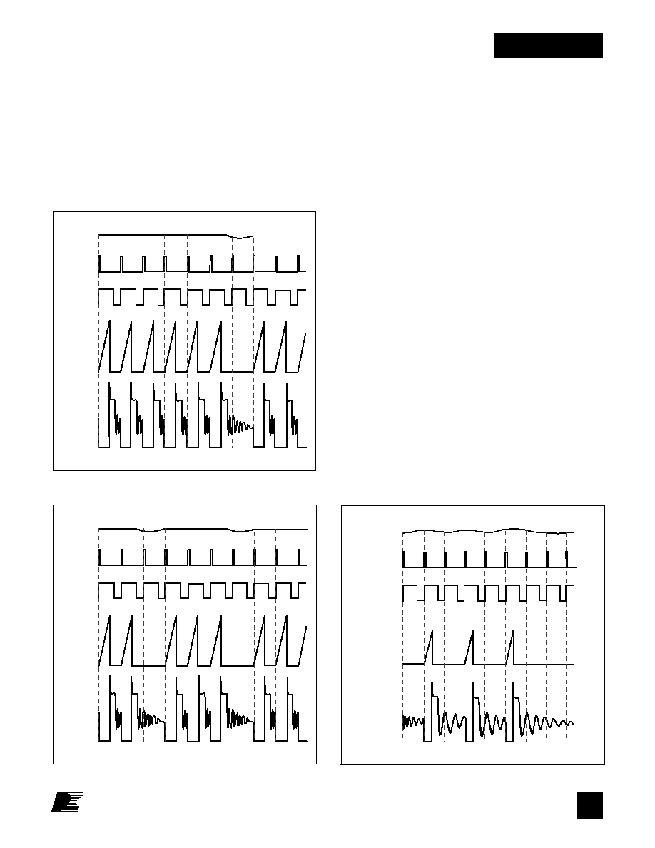
ON/OFF Operation with Current Limit State Machine
The internal clock of the TinySwitch-II runs all the time. At the
beginning of each clock cycle, it samples the EN/UV pin to
decide whether or not to implement a switch cycle, and based
on the sequence of samples over multiple cycles, it determines
the appropriate current limit. At high loads, when the EN/UV
pin is high (less than 240
µA out of the pin), a switching cycle
with the full current limit occurs. At lighter loads, when EN/UV
is high, a switching cycle with a reduced current limit occurs.
At near maximum load, TinySwitch-II will conduct during
nearly all of its clock cycles (Figure 6). At slightly lower load,
it will "skip" additional cycles in order to maintain voltage
regulation at the power supply output (Figure 7). At medium
loads, cycles will be skipped and the current limit will be
reduced (Figure8). At very light loads, the current limit will be
reduced even further (Figure 9). Only a small percentage of
cycles will occur to satisfy the power consumption of the power
supply.
The response time of the TinySwitch-II ON/OFF control scheme
is very fast compared to normal PWM control. This provides
tight regulation and excellent transient response.
Power Up/Down
The TinySwitch-II requires only a 0.1
µF capacitor on the
BYPASS pin. Because of its small size, the time to charge this
capacitor is kept to an absolute minimum, typically 0.6 ms. Due
to the fast nature of the ON/OFF feedback, there is no overshoot
at the power supply output. When an external resistor (2 M
) is
connected from the positive DC input to the EN/UV pin, the power
MOSFET switching will be delayed during power-up
until the DC line voltage exceeds the threshold (100 V). Figures
10 and 11 show the power-up timing waveform of TinySwitch-II
Figure 6. TinySwitch-II Operation at Near Maximum Loading.
V
DRAIN
V
EN
CLOCK
D
DRAIN
I
MAX
PI-2667-090700
Figure 8. TinySwitch-II Operation at Medium Loading.
PI-2377-091100
V
DRAIN
V
EN
CLOCK
D
DRAIN
I
MAX
Figure 7. TinySwitch-II Operation at Moderately Heavy Loading.

6
B
7/01
TNY264/266-268
Figure 12. Normal Power-down Timing (without UV).
Figure 13. Slow Power-down Timing with Optional External
(2 M
) UV Resistor Connected to EN/UV Pin.
PI-2395-030801
0
2.5
5
Time (s)
0
100
200
400
300
0
100
200
V
DC-INPUT
V
DRAIN
in applications with and without an external resistor (2 M
)
connected to the EN/UV pin.
During power-down, when an external resistor is used, the
power MOSFET will switch for 50 ms after the output loses
regulation. The power MOSFET will then remain off without
any glitches since the under-voltage function prohibits restart
when the line voltage is low.
Figure 12 illustrates a typical power-down timing waveform of
TinySwitch-II. Figure 13 illustrates a very slow power-down
timing waveform of TinySwitch-II as in standby applications.
The external resistor (2 M
) is connected to the EN/UV pin in
this case to prevent unwanted restarts.
Figure 10. TinySwitch-II Power-up with Optional External UV
Resistor (2 M
) Connected to EN/UV Pin.
Figure 11. TinySwitch-II Power-up without Optional External UV
Resistor Connected to EN/UV Pin.
PI-2381-1030801
0
1
2
Time (ms)
0
200
400
5
0
10
0
100
200
V
DC-INPUT
V
BYPASS
V
DRAIN
0
1
2
Time (ms)
0
200
400
5
0
10
0
100
200
PI-2383-030801
V
DC-INPUT
V
BYPASS
V
DRAIN
PI-2661-072400
V
DRAIN
V
EN
CLOCK
D
DRAIN
I
MAX
Figure 9. TinySwitch-II Operation at Very Light Load.
PI-2348-030801
0
.5
1
Time (s)
0
100
200
300
0
100
200
400
V
DC-INPUT
V
DRAIN
7
B
7/01
TNY264/266-268
Figure 14. 2.5 W Constant Voltage, Constant Current Battery Charger with Universal Input (85-265 VAC).
The TinySwitch-II does not require a bias winding to provide
power to the chip, because it draws the power directly from the
DRAIN pin (see Functional Description above). This has two
main benefits. First, for a nominal application, this eliminates
the cost of a bias winding and associated components.
Secondly, for battery charger applications, the current-voltage
characteristic often allows the output voltage to fall close to
zero volts while still delivering power. This type of application
normally requires a forward-bias winding which has many
more associated components. With TinySwitch-II, neither are
necessary. For applications that require a very low no-load
power consumption (50 mW), a resistor from a bias winding to
the BYPASS pin can provide the power to the chip. The
minimum recommended current supplied is 750
µA. The
BYPASS pin in this case will be clamped at 6.3 V. This method
will eliminate the power draw from the DRAIN pin, thereby
reducing the no-load power consumption and improving full-
load efficiency.
Current Limit Operation
Each switching cycle is terminated when the DRAIN current
reaches the current limit of the TinySwitch-II. Current limit
operation provides good line ripple rejection and relatively
constant power delivery independent of input voltage.
BYPASS Pin Capacitor
The BYPASS pin uses a small 0.1
µF ceramic capacitor for
decoupling the internal power supply of the TinySwitch-II.
Application Examples
The TinySwitch-II is ideal for low cost, high efficiency power
supplies in a wide range of applications such as cellular phone
chargers, PC standby, TV standby, AC adapters, motor control,
appliance control and ISDN or a DSL network termination. The
132 kHz operation allows the use of a low cost EE13 or EF12.6
core transformer while still providing good efficiency. The
frequency jitter in TinySwitch-II makes it possible to use a
single inductor (or two small resistors for under 3 W applications
if lower efficiency is acceptable) in conjunction with two input
capacitors for input EMI filtering. The auto-restart function
removes the need to oversize the output diode for short circuit
conditions allowing the design to be optimized for low cost and
maximum efficiency. In charger applications, it eliminates the
need for a second optocoupler and Zener diode for open loop
fault protection. Auto-restart also saves the cost of adding a fuse
or increasing the power rating of the current sense resistors to
survive reverse battery conditions. For applications requiring
under-voltage lock out (UVLO), such as PC standby, the
TinySwitch-II eliminates several components and saves cost.
TinySwitch-II is well suited for applications that require
constant voltage and constant current output. As TinySwitch-II
is always powered from the input high voltage, it therefore
does not rely on bias winding voltage. Consequently this greatly
simplifies designing chargers that must work down to zero volts
on the output.
PI-2706-052301
+ 5 V
500 mA
RTN
D1
1N4005
C1
3.3
µ
F
400 V
Fusible
RF1
8.2
C3
0.1
µ
F
C7
10
µ
F
10 V
85-265
VAC
L1
2.2 mH
D2
1N4005
D3
1N4005
D4
1N4005
R2
200 k
U2
LTV817
D5
1N5819
Shield
L2
3.3
µ
H
C5
330
µ
F
16 V
C2
3.3
µ
F
400 V
C6
100
µ
F
35 V
R7
100
R4
1.2
1/2 W
Q1
2N3904
R8
270
VR1
BZX79-
B3V9
3.9 V
U1
TNY264
C3
2.2 nF
D6
1N4937
R6
1
1/2 W
T1
R1
1.2 k
1
8
4
5
R3
22
R9
47
C8 680 pF
Y1 Safety
TinySwitch-II
D
S
BP
EN/UV

8
B
7/01
TNY264/266-268
2.5 W CV/CC Cell-Phone Charger
As an example, Figure 14 shows a TNY264 based 5 V, 0.5 A,
cellular phone charger operating over a universal input range
(85-265 VAC). The inductor (L1) forms a
-filter in conjunction
with C1 and C2. The resistor R1 damps resonances in the
inductor L1. Frequency jittering operation of TinySwitch-II
allows the use of a simple
-filter described above in combination
with a single low value Y1-capacitor (C8) to meet worldwide
conducted EMI standards. The addition of a shield winding in
the transformer allows conducted EMI to be met even with the
output capacitively earthed (which is the worst case condition
for EMI). The diode D6, capacitor C3 and resistor R2 comprise
the clamp circuit, limiting the leakage inductance turn-off
voltage spike on the TinySwitch-II DRAIN pin to a safe value.
The output voltage is determined by the sum of the optocoupler
U2 LED forward drop (~1 V), and Zener diode VR1 voltage.
Resistor R8 maintains a bias current through the Zener diode to
ensure it is operated close to the Zener test current.
A simple constant current circuit is implemented using the V
BE
of transistor Q1 to sense the voltage across the current sense
resistor R4. When the drop across R4 exceeds the V
BE
of
transistor Q1, it turns on and takes over control of the loop by
driving the optocoupler LED. Resistor R6 assures sufficient
voltage to keep the control loop in operation down to zero volts
at the output. With the output shorted, the drop across R4 and
R6 (~1.2 V) is sufficient to keep the Q1 and LED circuit active.
Resistors R7 and R9 limit the forward current that could be
drawn through VR1 by Q1 under output short circuit conditions,
due to the voltage drop across R4 and R6.
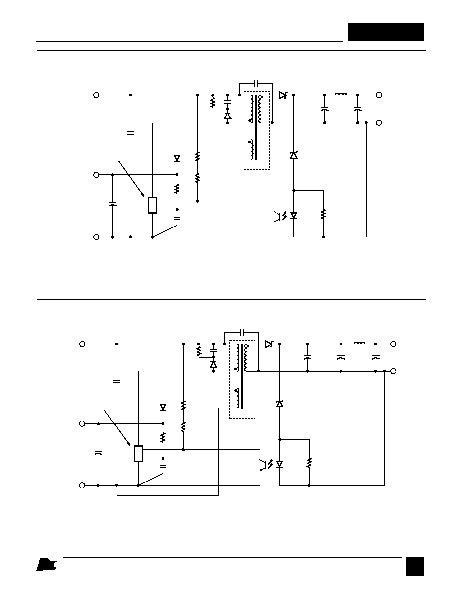
10 and 15 W PC Standby Circuits
Figures 15 and 16 show examples of circuits for PC standby
applications. They both provide two outputs: an isolated 5 V
and a 12V primary referenced output. The first, using TNY266P,
provides 10W, and the second, using TNY267P, 15 W of
output power. Both operate from an input range of 140 to
375VDC, corresponding to a 230 VAC or 100/115 VAC with
doubler input. The designs take advantage of the line under-
voltage detect, auto-restart and higher switching frequency of
TinySwitch-II. Operation at 132 kHz allows the use of a smaller
and lower cost transformer core, EE16 for 10 W and EE22 for
15 W. The removal of pin 6 from the 8 pin DIP TinySwitch-II
packages provides a large creepage distance which improves
reliability in high pollution environments such as fan cooled
PC power supplies.
Capacitor C1 provides high frequency decoupling of the high
voltage DC supply, only necessary if there is a long trace length
from the DC bulk capacitors of the main supply. The line sense
resistors R2 and R3 sense the DC input voltage for line under-
voltage. When the AC is turned off, the under-voltage detect
feature of the TinySwitch-II prevents auto-restart glitches at the
output caused by the slow discharge of large storage capacitance
in the main converter. This is achieved by preventing the
TinySwitch-II from switching when the input voltage goes
below a level needed to maintain output regulation, and keeping
it off until the input voltage goes above the under-voltage
threshold, when the AC is turned on again. With R2 and R3,
giving a combined value of 4 M
, the power up under-voltage
threshold is set at 200 VDC, slightly below the lowest required
operating DC input voltage, for start-up at 170 VAC, with
doubler. This feature saves several components needed to
implement the glitch-free turn-off compared with discrete or
TOPSwitch-II based designs. During turn-on the rectified DC
input voltage needs to exceed 200 V under-voltage threshold
for the power supply to start operation. But, once the power
supply is on it will continue to operate down to 140 V rectified
DC input voltage to provide the required hold up time for the
standby output.
The auxiliary primary side winding is rectified and filtered by
D2 and C2 to create a 12 V primary bias output voltage for the
main power supply primary controller. In addition, this voltage
is used to power the TinySwitch-II via R4. Although not
necessary for operation, supplying the TinySwitch-II externally
reduces the device quiescent dissipation by disabling the internal
drain derived current source normally used to keep the BYPASS
pin capacitor (C3) charged. An R4 value of 10 k
provides
600
µA into the BYPASS pin, which is slightly in excess of the
current consumption of TinySwitch-II. The excess current is
safely clamped by an on-chip active Zener diode to 6.3 V.
The secondary winding is rectified and filtered by D3 and C6.
For a 15W design an additional output capacitor, C7, is
required due to the larger secondary ripple currents compared
to the 10W PC standby design. The auto-restart function limits
output current during short circuit conditions, removing the
need to over rate D3. Switching noise filtering is provided by L1
and C8. The 5V output is sensed by U2 and VR1. R5 is used to
ensure that the Zener diode is biased at its test current.
The Zener regulation method provides sufficient accuracy (typ.
± 3%). This is possible because TinySwitch-II limits the
dynamic range of the optocoupler LED current, allowing the
Zener diode to operate at near constant bias current.
9
B
7/01
TNY264/266-268
C1
0.01
µ
F
1 kV
140-375
VDC
INPUT
L1
10
µ
H
2 A
R5
150
D3
1N5822
U1
TNY266P
C5
2.2 nF
1 kV
D1
1N4005
U2
SFH615-2
VR1
BZX79B3V9
5
4
2
1
10
8
TinySwitch-II
D
S
BP
+5 V
(
±
5%)
2 A
RTN
C2
82
µ
F
35 V
C8
470
µ
F
10 V
PI-2713-040901
C4
1 nF Y1
D2
1N4148
EN
+12 VDC
20 mA
0 V
C3
0.1
µ
F
50 V
R4
10 k
C6
1000
µ
F
10 V
R2
2 M
R3
2 M
R1
200 k
T1
PERFORMANCE SUMMARY
Continuous Output Power:
10.24 W
Efficiency:
75%
Figure 16. 15 W PC Standby Supply.
C1
0.01
µ
F
1 kV
140-375
VDC
INPUT
L1
10
µ
H
3 A
R5
150
D3
SB540
U1
TNY267P
C5
2.2 nF
1 kV
D1
1N4005
U2
SFH615-2
VR1
BZX79B3V9
PERFORMANCE SUMMARY
Continuous Output Power:
15.24 W
Efficiency:
78%
5
4
2
1
10
8
TinySwitch-II
D
S
BP
+5 V
(
±
5%)
3 A
RTN
C2
82
µ
F
35 V
C8
470
µ
F
10 V
PI-2712-040901
C4
1 nF Y1
D2
1N4148
EN
+12 VDC
20 mA
0 V
C3
0.1
µ
F
50 V
R4
10 k
C7
1000
µ
F
10 V
C6
1000
µ
F
10 V
R2
2 M
R3
2 M
R1
100 k
T1
Figure 15. 10 W PC Standby Supply.

10
B
7/01
TNY264/266-268
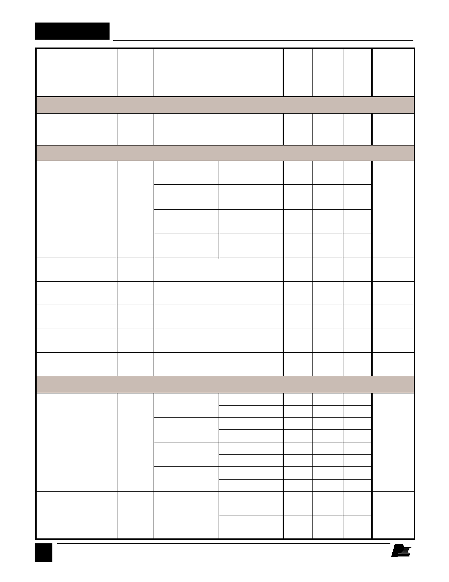
Key Application Considerations
TinySwitch-II
vs.
TinySwitch
Table 2 compares the features and performance differences
between the TNY254 device of the TinySwitch family with the
TinySwitch-II family of devices. Many of the new features
Table 2. Comparison Between TinySwitch and TinySwitch-II.
*Not available.
** See typical performance curves.
Function
TinySwitch
TinySwitch-II
TinySwitch-II
Advantages
TNY254
TNY264/266-268
Switching Frequency 44 kHz
±
10% (@25
∞
C) 132 kHz
±
6% (@25
∞
C) ∑ Smaller transformer for low cost
and Tolerance
∑ Ease of design
Temperature Variation +8%
+2%
∑ Manufacturability
(0 - 100
∞
C)**
∑ Optimum design for lower cost
Active Frequency Jitter
N/A*
±
4 kHz
∑ Lower EMI minimizing filter
component costs
Transformer
N/A*
Yes - built into
∑ Practically eliminates audible noise
Audible Noise
controller
with ordinary dip varnished
Reduction
transformer ≠ no special construction
or gluing required
Line UV Detect
N/A*
Single resistor
∑ Prevents power on/off glitches
programmable
Current Limit Tolerance
±
11% (@25
∞
C)
±
7% (@25
∞
C)
∑ Increases power capability and
Temperature Variation
-8%
0%
simplifies design for high volume
(0 - 100
∞
C)**
manufacturing
Auto-Restart
N/A*
6% effective on-time
∑ Limits output short-circuit current to
less than full load current
- No output diode size penalty.
∑ Protects load in open loop fault
conditions
- No additional components
required
BYPASS Pin
N/A*
Internally clamped to
∑ Allows TinySwitch-II to be powered
Zener Clamp
6.3 V
from a low voltage bias winding to
improve efficiency and to reduce
on-chip power dissipation
DRAIN Creepage at
0.037" / 0.94 mm
0.137" / 3.48 mm
∑ Greater immunity to arcing as a
Package
result of dust, debris or other
contaminants build-up
Design
Output Power
Table 1 (front page) shows the practical maximum continuous
output power levels that can be obtained under the following
conditions:
1. The minimum DC input voltage is 90 V or higher for
85 VAC input, or 240 V or higher for 230 VAC input or
115 VAC input with a voltage doubler. This corresponds to
a filter capacitor of 3
µF/W for universal input and 1 µF/W
for 230 or 115 VAC with doubler input.
eliminate the need for or reduce the cost of circuit components.
Other features simplify the design and enhance performance.

11
B
7/01
TNY264/266-268
2. A secondary output of 5 V with a Schottky rectifier diode.
3. Assumed efficiency of 77% (TNY267 & TNY268), 75%
(TNY266) and 73% (TNY264).
4. The parts are board mounted with SOURCE pins soldered
to sufficient area of copper to keep the die temperature at or
below 100
∞C.
In addition to the thermal environment (sealed enclosure,
ventilated, open frame, etc.), the maximum power capability of
TinySwitch-II in a given application depends on transformer
core size and design (continuous or discontinuous), efficiency,
minimum specified input voltage, input storage capacitance,
output voltage, output diode forward drop, etc., and can be
different from the values shown in Table 1.
Audible Noise
The TinySwitch-II practically eliminates any transformer audio
noise using simple ordinary varnished transformer construction.
No gluing of the cores is needed. The audio noise reduction is
accomplished by the TinySwitch-II controller reducing the
current limit in discrete steps as the load is reduced. This
minimizes the flux density in the transformer when switching
at audio frequencies.
Worst Case EMI & Efficiency Measurement
Since identical TinySwitch-II supplies may operate at several
different frequencies under the same load and line conditions,
care must be taken to ensure that measurements are made under
worst case conditions. When measuring efficiency or EMI
verify that the TinySwitch-II is operating at maximum frequency
and that measurements are made at both low and high line input
voltages to ensure the worst case result is obtained.
Layout
Single Point Grounding
Use a single point ground connection at the SOURCE pin for
the BYPASS pin capacitor and the Input Filter Capacitor
(see Figure 17).
Primary Loop Area
The area of the primary loop that connects the input filter
capacitor, transformer primary and TinySwitch-II together
should be kept as small as possible.
Primary Clamp Circuit
A clamp is used to limit peak voltage on the DRAIN pin at turn-
off. This can be achieved by using an RCD clamp (as shown in
Figure 14). A Zener and diode clamp (200 V) across the
primary or a single 550V Zener clamp from DRAIN to SOURCE
can also be used. In all cases care should be taken to minimize
the circuit path from the clamp components to the transformer
and TinySwitch-II.
Thermal Considerations
Copper underneath the TinySwitch-II acts not only as a single
point ground, but also as a heatsink. The hatched areas shown
in Figure17 should be maximized for good heat sinking of
TinySwitch-II and the same applies to the output diode.
EN/UV pin
If a line under-voltage detect resistor is used then the resistor
should be mounted as close as possible to the EN/UV pin to
minimize noise pick up.
The voltage rating of a resistor should be considered for the
under-voltage detect (Figure 15: R2, R3) resistors. For 1/4W
resistors, the voltage rating is typically 200V continuous,
whereas for 1/2W resistors the rating is typically 400V
continuous.
Y-Capacitor
The placement of the Y-capacitor should be directly from the
primary bulk capacitor positive rail to the common/return
terminal on the secondary side. Such placement will maximize
the EMI benefit of the Y-capacitor and avoid problems in
common-mode surge testing.
Optocoupler
It is important to maintain the minimum circuit path from the
optocoupler transistor to the TinySwitch-II EN/UV and
SOURCE pins to minimize noise coupling.
The EN/UV pin connection to the optocoupler should be kept
to an absolute minimum (less than 12.7 mm or 0.5 in.), and
this connection should be kept away from the DRAIN pin
(minimum of 5.1 mm or 0.2 in.).
Output Diode
For best performance, the area of the loop connecting the
secondary winding, the Output Diode and the Output Filter
Capacitor, should be minimized. See Figure17 for optimized
layout. In addition, sufficient copper area should be provided
at the anode and cathode terminals of the diode for adequate
heatsinking.
Input and Output Filter Capacitors
There are constrictions in the traces connected to the input and
output filter capacitors. These constrictions are present for two
reasons. The first is to force all the high frequency currents to
flow through the capacitor (if the trace were wide then it could
flow around the capacitor). Secondly, the constrictions minimize
the heat transferred from the TinySwitch-II to the input filter
capacitor and from the secondary diode to the output filter
capacitor. The common/return (the negative output terminal in
Figure17) terminal of the output filter capacitor should be
connected with a short, low impedance path to the secondary
winding. In addition, the common/return output connection
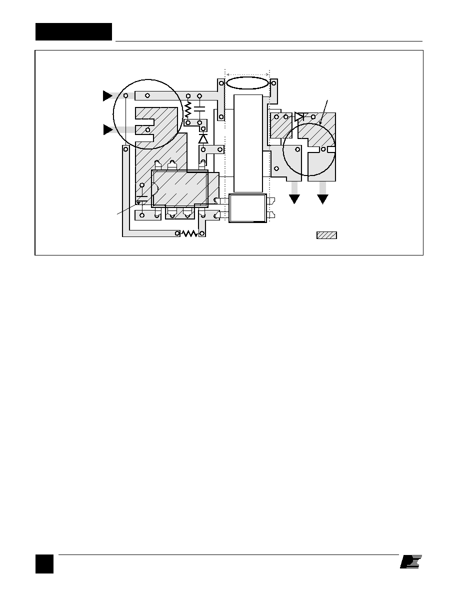
12
B
7/01
TNY264/266-268
TOP VIEW
PI-2707-012901
Y1-
Capacitor
Opto-
coupler
D
EN/UV
BP
+
--
HV
+
-- DC
Out
Input Filter Capacitor
Output Filter Capacitor
Safety Spacing
Maximize hatched copper
areas ( ) for optimum
heat sinking
S
S
SEC
C
BP
TinySwitch-II
PRI
T
r
a
n
s
f
o
r
m
e
r
Figure 17. Recommended Circuit Board Layout for TinySwitch-II with Under-Voltage Lock Out Resistor.
should be taken directly from the secondary winding pin and not
from the Y-capacitor connection point.
PC Board Cleaning
Power Integrations does not recommend the use of "no clean"
flux.
For the most up-to-date information visit the
PI Web site at: www.powerint.com

13
B
7/01
TNY264/266-268
BYPASS Voltage .......................................... -0.3 V to 9 V
Storage Temperature ..................................... -65 to 150
∞C
Operating Junction Temperature
(2)
................ -40 to 150
∞C
Lead Temperature
(3)
................................................ 260
∞C
Notes:
1. All voltages referenced to SOURCE, T
A
= 25
∞C.
2. Normally limited by internal circuitry.
3. 1/16" from case for 5 seconds.
ABSOLUTE MAXIMUM RATINGS
(1)
DRAIN Voltage ....................................... - 0.3 V to 700 V
Peak DRAIN Current (TNY264) ...........................400 mA
Peak DRAIN Current (TNY266) ...........................560 mA
Peak DRAIN Current (TNY267) ...........................720 mA
Peak DRAIN Current (TNY268) ...........................880 mA
EN/UV Voltage ............................................ - 0.3 V to 9 V
EN/UV Current ......................................................100 mA
CONTROL FUNCTIONS
Output
Frequency
Maximum
Duty Cycle
EN/UV Pin Turnoff
Threshold Current
EN/UV Pin
Voltage
DRAIN
Supply Current
BYPASS Pin
Charge Current
BYPASS Pin
Voltage
BYPASS Pin
Voltage Hysteresis
kHz
%
µ
A
V
µ
A
µ
A
mA
V
Min
Typ
Max
f
OSC
DC
MAX
I
DIS
V
EN
I
S1
I
S2
I
CH1
I
CH2
V
BP
V
BPH
Parameter
Symbol
(Unless Otherwise Specified)
See Figure 18
Conditions
170
225
270
-7.5
-4.6
-2.5
T
J
= 25
∞
C
See Figure 4
Units
SOURCE = 0 V
;
T
J
= -40 to 125
∞
C
62
65
68
T
J
= -40
∞
C to 125
∞
C
V
BP
= 0 V,
T
J
= 25
∞
C
See Note C, D
320
430
500
Average
Peak-Peak Jitter
124
132
140
8
-300
-240
-170
0.4
1.0
1.5
-4.5
-3.0
-1.5
Notes:
1. Measured on the SOURCE pin close to plastic interface.
2. Soldered to 0.36 sq. inch (232 mm
2
), 2oz. (610 gm/m
2
) copper clad.
3. Soldered to 1 sq. inch (645 mm
2
), 2oz. (610 gm/m
2
) copper clad.
S1 Open
I
EN/UV
= -125
µ
A
V
EN/UV
= 0 V
V
BP
= 4 V,
T
J
= 25
∞
C
See Note C, D
I
EN/UV
= 25
µ
A
THERMAL IMPEDANCE
1.3
2.3
2.7
200
265
320
240
315
380
285
380
460
TNY264
TNY266
TNY267
5.6
5.85
6.15
0.80
0.95
1.20
See Note C
TNY268
V
Thermal Impedance: P/G Package:
(
JA
) ........ 45
∞C/W
(2)
; 35
∞C/W
(3)
(
JC
)
(1)
.......................... 11
∞C/W
EN/UV Open
(MOSFET
Switching)
See Note A, B
-3.8
-2.0
-1.0
-5.5
-3.3
-1.8
TNY264
TNY266-268
TNY264
TNY266-268
14
B
7/01
TNY264/266-268
OUTPUT
T
J
= 25
∞
C
See Figure 21
T
J
= 25
∞
C
Conditions
Parameter
Symbol
SOURCE = 0 V; T
J
= -40 to 125
∞
C
See Figure 18
(Unless Otherwise Specified)
I
LUV
I
LIMIT
I
INIT
t
LEB
t
ILD
R
DS(ON)
I
DSS
Min
Typ
Max
Units
CONTROL FUNCTIONS (cont.)
V
BP
= 6.2 V,
V
EN/UV
= 0 V,
V
DS
= 560 V,
T
J
= 125
∞
C
T
J
= 25
∞
C
See Note F, G
T
J
= 25
∞
C
See Note F
TNY264
T
J
= 25
∞
C
49
54
44
µ
A
CIRCUIT PROTECTION
mA
mA
ns
ns
∞
C
∞
C
µ
A
233
250
267
170
215
150
125
135
150
70
28
32
42
48
14
16
50
100
0.65 x
I
LIMIT (MIN)
EN/UV Pin Line
Under-voltage
Threshold
Current Limit
Initial Current
Limit
Leading Edge
Blanking Time
Current Limit
Delay
Thermal Shutdown
Temperature
Thermal Shutdown
Hysteresis
ON-State
Resistance
OFF-State
Leakage
325
350
375
419
450
481
512
550
588
di/dt = 50 mA/
µ
s
See Note E
21
24
7.8
9.0
11.7
13.5
5.2
6.0
7.8
9.0
TNY266
T
J
= 25
∞
C
TNY267
T
J
= 25
∞
C
TNY268
T
J
= 25
∞
C
di/dt = 70 mA/
µ
s
See Note E
di/dt = 90 mA/
µ
s
See Note E
di/dt = 110 mA/
µ
s
See Note E
TNY264
I
D
= 25 mA
T
J
= 25
∞
C
T
J
= 100
∞
C
T
J
= 25
∞
C
T
J
= 100
∞
C
T
J
= 25
∞
C
T
J
= 25
∞
C
T
J
= 100
∞
C
TNY266
I
D
= 35 mA
TNY267
I
D
= 45 mA
TNY268
I
D
= 55 mA
T
J
= 100
∞
C
TNY264
TNY266
TNY267
TNY268

15
B
7/01
TNY264/266-268
NOTES:
A. Total current consumption is the sum of I
S1
and I
DSS
when EN/UV pin is shorted to ground (MOSFET not switching)
and the sum of I
S2
and I
DSS
when EN/UV pin is open (MOSFET switching).
B Since the output MOSFET is switching, it is difficult to isolate the switching current from the supply current at the
DRAIN. An alternative is to measure the BYPASS pin current at 6.1 V.
C. BYPASS pin is not intended for sourcing supply current to external circuitry.
D. See typical performance characteristics section for BYPASS pin start-up charging waveform.
E. For current limit at other di/dt values, refer to Figure 25.
F. This parameter is derived from characterization.
G. This parameter is derived from the change in current limit measured at 1X and 4X of the di/dt shown in the I
LIMIT
specification.
H. Auto-restart on time has the same temperature characteristics as the oscillator (inversely proportional to
frequency).
Conditions
Parameter
Symbol
SOURCE = 0 V; T
J
= -40 to 125
∞
C
See Figure 18
(Unless Otherwise Specified)
10
V
µ
s
µ
s
ms
%
Drain Supply
Voltage
Output EN/UV
Delay
Output Disable
Setup Time
Min
Typ
Max
Units
OUTPUT (cont.)
Auto-Restart
ON-Time
Auto-Restart
Duty Cycle
t
AR
DC
AR
0.5
50
T
J
= 25
∞
C
See Note H
t
DST
t
EN/UV
5.6
See Figure 20
50
Measured in a Typical Flyback
Converter Application
50
50
V
ns
ns
t
F
t
R
Rise Time
Fall Time
700
V
BP
= 6.2 V, V
EN/UV
= 0 V,
I
DS
= 100
µ
A, T
J
= 25
∞
C
BV
DSS
Breakdown
Voltage
16
B
7/01
TNY264/266-268
Figure 19. TinySwitch-II Duty Cycle Measurement.
Figure 20. TinySwitch-II Output Enable Timing.
PI-2048-033001
DRAIN
VOLTAGE
HV
0 V
90%
10%
90%
t2
t1
D =
t1
t2
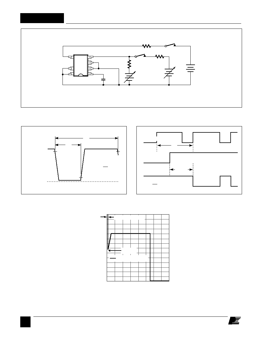
Figure 18. TinySwitch-II General Test Circuit.
PI-2686-101700
0.1
µ
F
10 V
50 V
470
5 W
S2
470
NOTE: This test circuit is not applicable for current limit or output characteristic measurements.
D EN/UV
BP
S
S
S
S
150 V
S1
2 M
PI-2364-012699
EN/UV
tP
tEN/UV
DC
MAX
t
P
=
1
f
OSC
V
DRAIN
(internal signal)
0.8
1.3
1.2
1.1
0.9
0.8
1.0
0
0
1
2
6
8
3
Time (
µ
s)
DRAIN Current (normalized)
PI-2362-052301
4
5
7
0.7
0.6
0.5
0.4
0.3
0.2
0.1
ILIMIT(MIN) @ 100
∞
C
IINIT(MIN)
tLEB (Blanking Time)
Figure 21. Current Limit Envelope.
17
B
7/01
TNY264/266-268
Typical Performance Characteristics
Figure 22. Breakdown vs. Temperature.
1.1
1.0
0.9
-50 -25
0
25
50
75 100 125 150
Junction Temperature (
∞
C)
Breakdown Voltage
(Normalized to 25
∞
C)
PI-2213-012301
1.2
1.0
0.8
0.6
0.4
0.2
0
-50
-25
0
25
50
75
100 125
Junction Temperature (
∞
C)
PI-2680-012301
Output Frequency
Normalized to 25
∞
C
6
5
4
3
2
1
0
0
0.2
0.4
0.6
0.8
1.0
Time (ms)
PI-2240-012301
BYPASS Pin Voltage (V)
7
Drain Voltage (V)
Drain Current (mA)
300
250
200
100
50
150
0
0
2
4
6
8
10
T
CASE
=25
∞
C
T
CASE
=100
∞
C
PI-2221-031401
TNY264
1.0
TNY266
2.0
TNY267
3.5
TNY268
5.5
Scaling Factors:
Figure 23. Frequency vs. Temperature.
Figure 24. Current Limit vs. Temperature.
Figure 25. Current Limit vs. di/dt.
Figure 26. Bypass Pin Start-up Waveform.
Figure 27. Output Characteristic.
1.4
1.2
1.0
0.8
0.6
0.4
0.2
0
1
2
3
4
Normalized di/dt
PI-2697-012301
Normalized Current Limit
TNY264 50 mA/
µ
s 250 mA
TNY266 70 mA/
µ
s 350 mA
TNY267 90 mA/
µ
s 450 mA
TNY268 110 mA/
µ
s 550 mA
Normalized
di/dt = 1
Normalized
Current
Limit = 1
1
0.8
0.6
0.4
0.2
0
-50
0
50
100
150
Temperature (
∞
C)
PI-2714-031401
1.2
Current Limit
(Normalized to 25
∞
C)
TNY264/266
TNY267
TNY268
18
B
7/01
TNY264/266-268
Typical Performance Characteristics (cont.)
TinySwitch Product Family
Series Number
Package Identifier
G
Plastic Surface Mount DIP
P
Plastic DIP
Package/Lead Options
Blank
Standard Configurations
TL
Tape & Reel, 1 k pcs minimum, G Package only
PART ORDERING INFORMATION
TNY 264 G - TL
Drain Voltage (V)
Drain Capacitance (pF)
PI-2683-031401
0
100
200
300
400
500
600
1
10
100
1000
TNY264
1.0
TNY266
2.0
TNY267
3.5
TNY268
5.5
Scaling Factors:
35
20
25
30
5
10
15
0
0
200
400
600
Drain Voltage (V)
Power (mW)
PI-2225-031401
TNY264
1.0
TNY266
2.0
TNY267
3.5
TNY268
5.5
Scaling Factors:
1.2
1.0
0.8
0.6
0.4
0.2
0
-50
-25
0
25
50
75
100 125
Junction Temperature (
∞
C)
PI-2698-012301
Under-Voltage Threshold
(Normalized to 25
∞
C)
Figure 28. C
OSS
vs. Drain Voltage.
Figure 29. Drain Capacitance Power.
Figure 30. Undervoltage Threshold vs. Temperature.
19
B
7/01
TNY264/266-268
Notes:
1. Package dimensions conform to JEDEC specification
MS-001-AB (Issue B 7/85) for standard dual-in-line (DIP)
package with .300 inch row spacing.
2. Controlling dimensions are inches. Millimeter sizes are
shown in parentheses.
3. Dimensions shown do not include mold flash or other
protrusions. Mold flash or protrusions shall not exceed
.006 (.15) on any side.
4. Pin locations start with Pin 1, and continue counter-clock-
wise to Pin 8 when viewed from the top. The notch and/or
dimple are aids in locating Pin 1. Pin 6 is omitted.
5. Minimum metal to metal spacing at the package body for
the omitted lead location is .137 inch (3.48 mm).
6. Lead width measured at package body.
7. Lead spacing measured with the leads constrained to be
perpendicular to plane T.
.010 (.25)
.015 (.38)
.300 (7.62) BSC
(NOTE 7)
.300 (7.62)
.390 (9.91)
.375 (9.53)
.385 (9.78)
.245 (6.22)
.255 (6.48)
.128 (3.25)
.132 (3.35)
.057 (1.45)
.063 (1.60)
.125 (3.18)
.135 (3.43)
0.15 (.38)
MINIMUM
.048 (1.22)
.053 (1.35)
.100 (2.54) BSC
.014 (.36)
.022 (.56)
-E-
Pin 1
SEATING
PLANE
-D-
-T-
P08B
DIP-8B
PI-2551-101599
D S .004 (.10)
T E D S .010 (.25) M
(NOTE 6)
SMD-8B
PI-2546-040501
.004 (.10)
.012 (.30)
.036 (0.91)
.044 (1.12)
.004 (.10)
0 -
∞
8
∞
.375 (9.53)
.385 (9.78)
.048 (1.22)
.009 (.23)
.053 (1.35)
.032 (.81)
.037 (.94)
.128 (3.25)
.132 (3.35)
-D-
Notes:
1. Controlling dimensions are
inches. Millimeter sizes are
shown in parentheses.
2. Dimensions shown do not
include mold flash or other
protrusions. Mold flash or
protrusions shall not exceed
.006 (.15) on any side.
3. Pin locations start with Pin 1,
and continue counter-clock
Pin 8 when viewed from the
top. Pin 6 is omitted.
4. Minimum metal to metal
spacing at the package body
for the omitted lead location
is .137 inch (3.48 mm).
5. Lead width measured at
package body.
6. D and E are referenced
datums on the package
body.
.057 (1.45)
.063 (1.60)
(NOTE 5)
E S
.100 (2.54) (BSC)
.372 (9.45)
.245 (6.22)
.388 (9.86)
.255 (6.48)
.010 (.25)
-E-
Pin 1
D S .004 (.10)
G08B
Heat Sink is 2 oz. Copper
As Big As Possible
.420
.046 .060
.060 .046
.080
Pin 1
.086
.186
.286
Solder Pad Dimensions

20
B
7/01
TNY264/266-268
Notes
-
1) Corrected first page spacing and sentence in description describing innovative design.
2) Corrected Frequency Jitter in Figure 4 and Frequency Jitter in Parameter Table.
3) Added last sentence to Over Temperature Protection section.
4) Clarified detecting when there is no external resistor connected to the EN/UV pin.
5) Corrected Figure 6 and its description in the text.
6) Corrected formatting, grammer and style errors in text and figures.
7) Corrected and moved Worst Case EMI & Efficiency Measurement section
8) Added PC Board Cleaning section.
9) Replaced Figure 21 and SMD-8B Package Drawing.
Date
3/01
7/01
Revision
A
B
KOREA
Power Integrations
International Holdings, Inc.
Rm# 402, Handuk Building
649-4 Yeoksam-Dong,
Kangnam-Gu,
Seoul, Korea
Phone:
+82-2-568-7520
Fax:
+82-2-568-7474
e-mail: koreasales@powerint.com
WORLD HEADQUARTERS
AMERICAS
Power Integrations, Inc.
5245 Hellyer Avenue
San Jose, CA 95138 USA
Main:
+1 408-414-9200
Customer Service:
Phone:
+1 408-414-9665
Fax:
+1 408-414-9765
e-mail: usasales@powerint.com
For the latest updates, visit our Web site: www.powerint.com
Power Integrations reserves the right to make changes to its products at any time to improve reliability or manufacturability.
Power Integrations does not assume any liability arising from the use of any device or circuit described herein, nor does it
convey any license under its patent rights or the rights of others.
The PI Logo, TOPSwitch, TinySwitch and EcoSmart are registered trademarks of Power Integrations, Inc.
©Copyright 2001, Power Integrations, Inc.
JAPAN
Power Integrations, K.K.
Keihin-Tatemono 1st Bldg.
12-20 Shin-Yokohama 2-Chome
Kohoku-ku, Yokohama-shi
Kanagawa 222-0033, Japan
Phone:
+81-45-471-1021
Fax:
+81-45-471-3717
e-mail: japansales@powerint.com
TAIWAN
Power Integrations
International Holdings, Inc.
17F-3, No. 510
Chung Hsiao E. Rd.,
Sec. 5,
Taipei, Taiwan 110, R.O.C.
Phone:
+886-2-2727-1221
Fax:
+886-2-2727-1223
e-mail: taiwansales@powerint.com
EUROPE & AFRICA
Power Integrations (Europe) Ltd.
Centennial Court
Easthampstead Road
Bracknell
Berkshire, RG12 1YQ
United Kingdom
Phone:
+44-1344-462-300
Fax:
+44-1344-311-732
e-mail: eurosales@powerint.com
CHINA
Power Integrations
International Holdings, Inc.
Rm# 1705, Bao Hua Bldg.
1016 Hua Qiang Bei Lu
Shenzhen, Guangdong 518031
China
Phone:
+86-755-367-5143
Fax:
+86-755-377-9610
e-mail: chinasales@powerint.com
INDIA (Technical Support)
Innovatech
#1, 8th Main Road
Vasanthnagar
Bangalore, India 560052
Phone:
+91-80-226-6023
Fax:
+91-80-228-9727
e-mail: indiasales@powerint.com
APPLICATIONS HOTLINE
World Wide +1-408-414-9660
APPLICATIONS FAX
World Wide +1-408-414-9760